Science
Columbia Engineers Advance Quantum Technologies with Nanoscale Metasurfaces
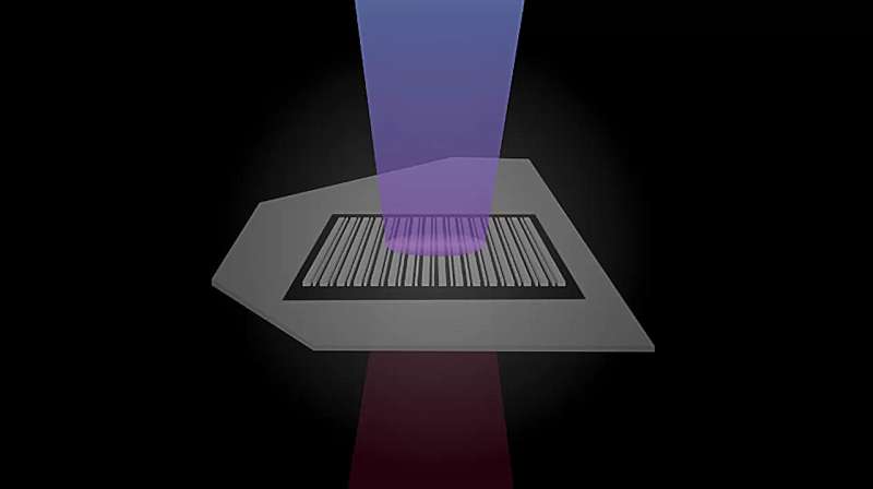
Researchers at Columbia University have made significant strides in quantum technology by developing a novel method to enhance nonlinear optical effects using ultrathin crystalline materials. Led by Jim Schuck, a professor of mechanical engineering, the team has successfully created a device just 3.4 micrometers thick that facilitates the generation of entangled photon pairs, a crucial component for advancing quantum technologies.
In a paper published in Nature Photonics in October, the team detailed how they reduced the dimensions of nonlinear platforms to an unprecedented 160 nanometers by employing metasurfaces—artificial geometries etched into 2D crystals. This innovation allows for improved optical properties and efficient generation of new frequencies of light.
Enhancing Nonlinearity in Quantum Devices
The research focuses on transition metal dichalcogenides (TMDs), a class of materials that can be thinned down to a single atom. Although these ultrathin layers exhibit high nonlinearity, they previously lacked the efficiency needed to produce photons at frequencies comparable to conventional nonlinear crystals commonly used in lasers. Chiara Trovatello, the corresponding author and currently an assistant professor at Politecnico di Milano, explained the significance of size in quantum technologies, stating, “For quantum processors, size becomes crucial.”
Current qubit sources, the building blocks of quantum devices, are often several centimeters in size, resulting in large, room-filling setups reminiscent of early classical computers. “To make quantum technologies scalable, we need to shrink the size of our qubit sources,” Trovatello added.
In January’s publication, the team utilized a method called periodic poling to optimize the optical output of a TMD called molybdenum disulfide. By layering the material in alternating directions, they ensured that light waves traveling through each layer were phase-matched, preventing interference.
Innovative Metasurface Design
The current research builds on this foundation by introducing a complementary platform featuring highly tunable, etched metasurfaces. Zhi Hao Peng, a doctoral student and the first author of the study, developed a nanofabrication technique that patterns a molybdenum disulfide flake with repeating lines. “Our design enhances the nonlinear effects much more than traditional linear optical optimization techniques, achieving strong enhancement not previously possible,” Peng noted.
The metasurface design improved second-harmonic generation by nearly 150 times compared to unpatterned materials. This process involves the merging of two photons to create one photon with double the frequency and half the wavelength of the original light particles. The researchers plan to reverse this process to split one photon into two entangled photons.
Schuck emphasized the significance of this technique, stating, “Nonlinear crystals have been key to many photonic technologies, but these materials can be brittle and difficult to fabricate. Peng figured out a deceptively simple technique that allows for increasingly complex patterns using standard cleanroom etching technologies.”
Collaborators from the CUNY Advanced Science Research Center, including Andrea Alu and former postdoctoral researcher Michele Cortufo, aided in determining the metasurface pattern needed to achieve macroscopic efficiencies across ultrathin path lengths. Cortufo explained, “We showed that such nontrivial behavior can be obtained with a remarkably simple modification to the sample.”
The combination of metasurfaces and 2D materials represents a pioneering step in photonics. Alu highlighted the potential, stating, “This work demonstrates how engineered nonlocalities in metasurfaces can unlock unprecedented nonlinear efficiencies.” The resulting light operates within telecommunications-range wavelengths, enhancing compatibility with current networks and devices.
As Schuck concluded, “This could be one of the most compact sources of entangled photons at that wavelength range. With our footprint, we can start to think about fully on-chip quantum photonics.”
For more detailed insights, the full study can be accessed in the article “3R-stacked transition metal dichalcogenide non-local metasurface for efficient second-harmonic generation” published in Nature Photonics.

Urgent Sewer Repairs Begin in Buffalo’s Fruit Belt Neighborhood

Leak Reveals Next-Gen Xbox Magnus as Premium Steam Machine

Trump Issues Ultimatum to Maduro; Venezuela Closes Airspace

Microsoft Faces Urgent Windows 11 Crisis Amid Core Failures

Engineering Legend Professor Ted de Winter Passes at 93

The Game Reacts to Celeste Rivas’ Death, Calls for Justice

Global Psoriasis Rates Climb Steadily, Especially in Wealthy Areas

$500,000 Grant Fuels Development of Children’s Imagination Station

OMERS Administration Corp Increases Stake in Qualcomm by 2.4%

Inventor Achieves Breakthrough with 2 Billion FPS Laser Video

Community Unites for 7th Annual Into the Light Walk for Mental Health

Charlie Sheen’s New Romance: ‘Glowing’ with Younger Partner

Dua Lipa Aces GCSE Spanish, Sparks Super Bowl Buzz with Fans

Mother Fights to Reunite with Children After Kidnapping in New Drama

Former Mozilla CMO Launches AI-Driven Cannabis Cocktail Brand Fast

Curium Group, PeptiDream, and PDRadiopharma Launch Key Cancer Trial

Tyler Technologies Set to Reveal Q3 Earnings on October 22

North Carolina’s Biotech Boom: Billions in New Investments
-
 Science1 month ago
Inventor Achieves Breakthrough with 2 Billion FPS Laser Video
-
 Health2 months ago
Community Unites for 7th Annual Into the Light Walk for Mental Health
-
 Top Stories2 months ago
Charlie Sheen’s New Romance: ‘Glowing’ with Younger Partner
-
 Entertainment2 months ago
Dua Lipa Aces GCSE Spanish, Sparks Super Bowl Buzz with Fans
-
 Entertainment2 months ago
Mother Fights to Reunite with Children After Kidnapping in New Drama
-
 Top Stories2 months ago
Former Mozilla CMO Launches AI-Driven Cannabis Cocktail Brand Fast
-
 Health2 months ago
Curium Group, PeptiDream, and PDRadiopharma Launch Key Cancer Trial
-
 Business2 months ago
Tyler Technologies Set to Reveal Q3 Earnings on October 22
-
 Health2 months ago
North Carolina’s Biotech Boom: Billions in New Investments
-

 World2 months ago
Israel Reopens Rafah Crossing After Hostage Remains Returned
-

 World2 months ago
R&B Icon D’Angelo Dies at 51, Leaving Lasting Legacy
-

 Entertainment2 months ago
Red Sox’s Bregman to Become Free Agent; Tigers Commit to Skubal