
Science
Backyard Shed Transformed into Class 100 Semiconductor Cleanroom

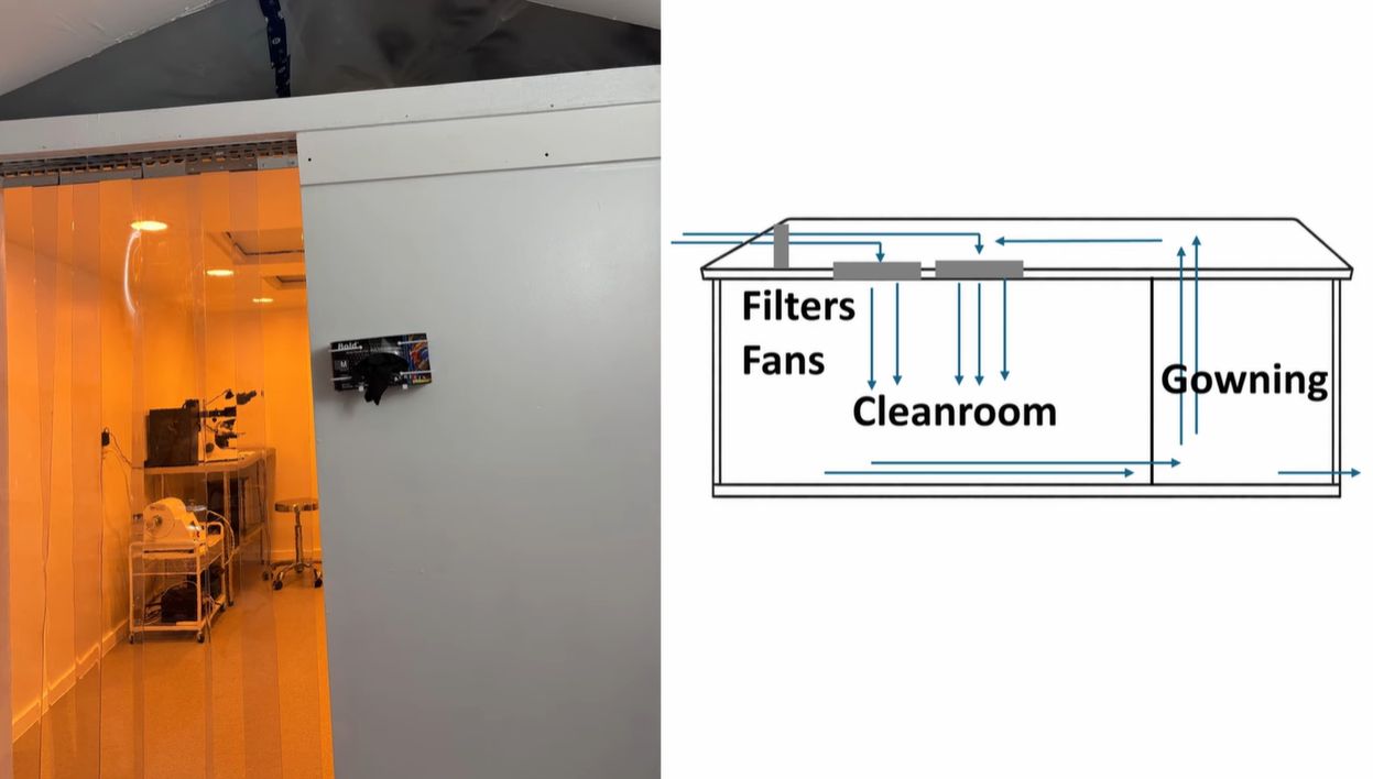
A typical garden shed has taken on a groundbreaking role in semiconductor research, thanks to the innovative efforts of Dr. Semiconductor. This project showcases how a simple backyard structure can be converted into a Class 100 cleanroom, meeting stringent standards necessary for semiconductor manufacturing.
The shed’s transformation begins with the implementation of high-efficiency particulate air (HEPA) filtration systems, which are critical for maintaining clean air. The design incorporates positive pressure to ensure clean air continuously flows into the space, preventing contaminants from entering. This approach mirrors the protocols used in multi-million-dollar semiconductor fabrication facilities, demonstrating that effective cleanroom technology can be both accessible and practical.
Inside the shed, the layout is thoughtfully divided. Upon entering, individuals first pass through a gowning room, where they don cleanroom attire before proceeding into the main cleanroom area. This careful transition helps to minimize contamination risks, which is crucial in semiconductor applications.
The cleanroom walls are outfitted with flame-resistant drywall, and a smooth, water-based epoxy coating has been applied to eliminate debris accumulation. This attention to detail contributes to a controlled environment where semiconductor research can thrive. The HEPA filtration system works in tandem with an air conditioning unit to maintain a stable temperature, essential for the sensitive nature of semiconductor materials.
Remarkably, measurements reveal that particle contamination levels within the shed align with a Federal Standard 209E equivalent of Class 100. This classification, which corresponds to ISO 5 standards, allows for a maximum of 3,520 particles/m³. In contrast, standard room air typically measures around ISO 9, with a staggering limit of 35,200,000 particles/m³. With these specifications, the shed meets the requirements necessary for research and development in semiconductor technologies, which is the primary focus of Dr. Semiconductor‘s YouTube channel.
This project exemplifies the potential for innovation in unexpected places, illustrating that high-tech solutions can emerge from humble origins. As individuals like Dr. Semiconductor explore unconventional avenues for research and development, the boundaries of semiconductor technology continue to expand.
Thanks to Thayer for bringing this remarkable story to light, showcasing how creativity and resourcefulness can redefine the landscape of technology.

Funko’s Price Target Increased to $4.00 as Analysts React

Humboldt Celebrates as ‘One Battle After Another’ Claims Best Picture

GSK Faces Backlash Over Asthma Inhaler Scrapping, Children Suffer

Adorable Sandhill Crane Colt Hugs Mom in The Villages

USA Unveils Star-Spangled Jerseys Ahead of March Friendlies

Newport Plans Colorful Lighting for Fourth Street Bridge

Sandia Scientists Honored for Innovative Career Journeys

Urgent: Charles M. Payment Passes Away at 78, Memorial Details Inside

NFL Free Agency: Key Moves and Player Signings in Week One

Researchers Launch $1.25M Project for Real-Time Hazard Monitoring in Hawaiʻi

Send It South Revives Culture and Community at The Momentary

UK Government Borrowing Hits £20.2 Billion in September Surge

Flipkart Republic Day Sale: iPhone 16 Plus Price Slashed by ₹23,900

Adecco SA Secures Mixed Ratings from Analysts Amid Earnings Update

Researchers Achieve Record 15.1 mA/cm² Hydrogen Production Efficiency

Globant Reveals Key Tech Forces Shaping Business in 2026

Inventor Achieves Breakthrough with 2 Billion FPS Laser Video

Dua Lipa Aces GCSE Spanish, Sparks Super Bowl Buzz with Fans
-
 Science8 months ago
Researchers Launch $1.25M Project for Real-Time Hazard Monitoring in Hawaiʻi
-
 Entertainment7 months ago
Send It South Revives Culture and Community at The Momentary
-
 World9 months ago
UK Government Borrowing Hits £20.2 Billion in September Surge
-
 Business6 months ago
Flipkart Republic Day Sale: iPhone 16 Plus Price Slashed by ₹23,900
-
 Sports7 months ago
Adecco SA Secures Mixed Ratings from Analysts Amid Earnings Update
-
 Top Stories5 months ago
Researchers Achieve Record 15.1 mA/cm² Hydrogen Production Efficiency
-
 Business8 months ago
Globant Reveals Key Tech Forces Shaping Business in 2026
-
 Science9 months ago
Inventor Achieves Breakthrough with 2 Billion FPS Laser Video
-
 Entertainment10 months ago
Dua Lipa Aces GCSE Spanish, Sparks Super Bowl Buzz with Fans
-

 Top Stories10 months ago
Charlie Sheen’s New Romance: ‘Glowing’ with Younger Partner
-

 Top Stories7 months ago
JSerra Names Hardy Nickerson as First Black Football Coach
-

 Health10 months ago
Community Unites for 7th Annual Into the Light Walk for Mental Health